Unpopulated (or De-Populated) Regions of PCBs

Discuss the development of new homebrew software, tools and libraries.

Moderators: cheriff, TyRaNiD

Post Reply
Dr. Vegetable
Posts: 171
Joined: Mon Nov 14, 2005 1:32 am
Location: Boston, Massachusetts
Contact:

Unpopulated (or De-Populated) Regions of PCBs

Post by Dr. Vegetable »

I have noticed many points on the PSP boards where there are traces to support components which are not actually mounted on the board. While this kind of thing is not uncommon in electrical hardware design, I sometimes wonder whether these areas are used when creating special PSPs to provide to registered developers, or whether some of these components are used during early manufacturing steps and removed later. Usually if components are never added to a board, there would be no solder on the traces, or the solder would be relatively smooth. In many cases, the solder is disturbed as if components had been removed after the PC boards were built.

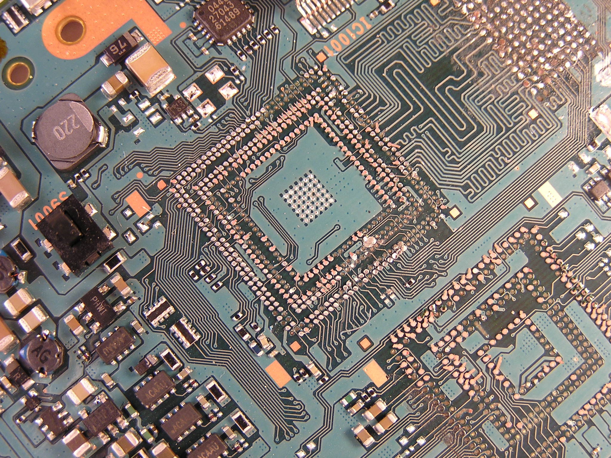
Two examples that actually look like very similar circuits can be found in these detail images. (Click the detail image to get PyroSama's original.)

Just north of the main CPU, this circuit appears to be able to connect to the circuit that runs the IrDA port, if it were populated with the right components. Especially interesting because of the four large test points in the middle of this area:
Image

Likewise, on the SIRCS/Wifi/Memory Stick daughterboard, there is another circuit that looks very similar:
Image

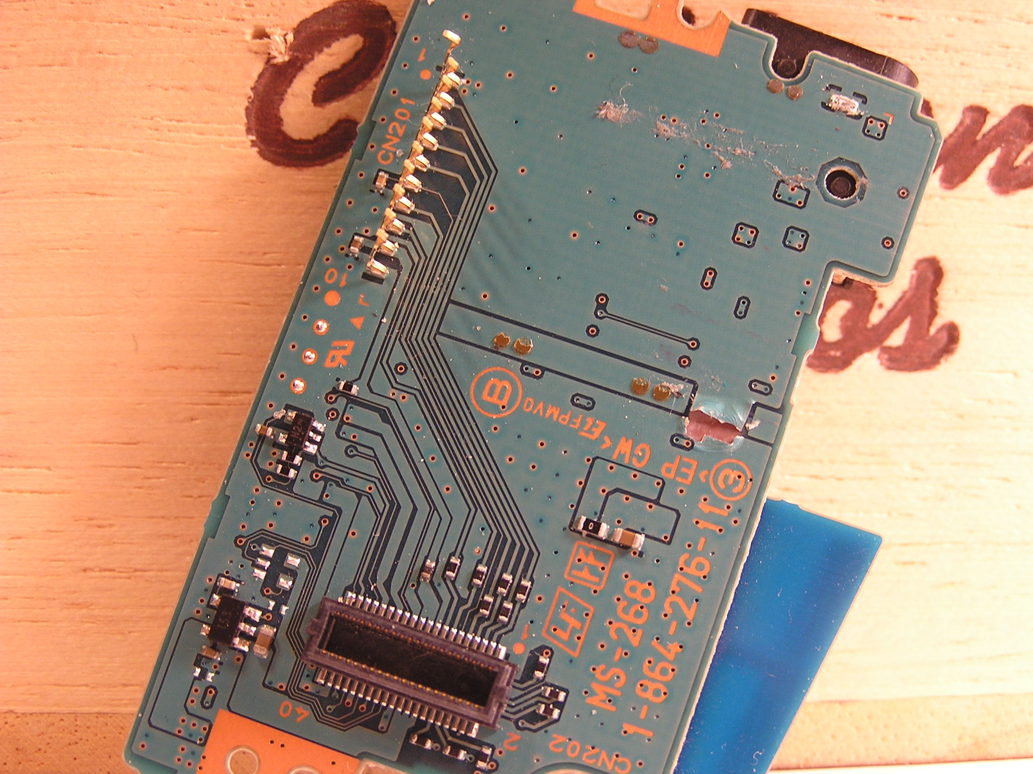
I haven't yet figured out what the 5-terminal devices are, but they look like they could be voltage regulators.

It is rumored that developers can load test code right onto the PSP through the SIRCS connector beside the headphone jack. It might make sense that a retail PSP would lack the physical hardware to make this possible. I want to trace these circuits out to see whether they show any promise. It might be possible to populate these circuits by hand (yes, I know some very good technicians!) and activate features that are not meant to be available to retail customers.

There are a few other places on the boards that have stuff like this going on as well.

Thanks again for the pictures, PyroSama! I always manage to notice something new every time I look at these that I have overlooked when studying the actual boards!

EDIT:
I might have gotten a bit circle-happy with that second image - the circle in the lower left actually is populated.

Not much info to go by on looking up those 5-terminal devices, but another possibility is that they are op-amps.
pyrosama
Posts: 66
Joined: Fri May 13, 2005 1:08 pm

Post by pyrosama »

Though those points are quite interesting and very numerous it wouldnt make much sence for sony to produce a board with all these extra points due to the slightly increased cost of production which when producing the volume of boards that they are would eventually add up, however it is hard to tell exactly.


Canti_
memon
Posts: 63
Joined: Mon Oct 03, 2005 10:51 pm

Post by memon »

Sotimes those duplivate pads/traces in PCBs are just because there are two types of component with same functionality but different size or pad configuration used for the same part of the circuit. The case below looks a bit like that to me.

Let's assume they are voltage regulators, then the bigger pads may belong to a 500mW version and the smaller to 100mW version. Sometimes one is cheaper than another (maybe even used for some other products in the same factory, etc), so it makes sense to allow to use both of them.

They propably use flow soldering for at least the passive components, so that's the reason all pads have some solder.

I would not get overly exited about that :)
Dr. Vegetable
Posts: 171
Joined: Mon Nov 14, 2005 1:32 am
Location: Boston, Massachusetts
Contact:

Post by Dr. Vegetable »

Perhaps. The bottom picture could be redundant circuitry, although I would expect more commonality between the traces if it were that simple.

I'm not getting too excited, but just presenting possibilities. Time will tell whether this is anything to get excited about.
mrn
Posts: 116
Joined: Wed Nov 02, 2005 2:26 am

Post by mrn »

from the back side, behind the UMD drive there are
2pcs of 4-pin and another two of 2-pin versions of the same stuff.
Dr. Vegetable
Posts: 171
Joined: Mon Nov 14, 2005 1:32 am
Location: Boston, Massachusetts
Contact:

Post by Dr. Vegetable »

An interesting possibility (unlikely though it may be) is that Sony inserts some kind of POGO board into the UMD drive that then makes contact with test points on the main board when the drive door is closed. So even though some of these test points are buried "deep inside", they could be easily accesed by someone with the right equipment.

That being said, those test points look kind of small for this type of use. POGO pins wouldn't make very good contact with tiny blobs of solder on a pad. Still, it makes me wonder how many other creative ways there are to get in there.

To borrow from an over-used catch-phrase: Keep on thinking outside the box about how to get inside the box...
User avatar
groepaz
Posts: 305
Joined: Thu Sep 01, 2005 7:44 am
Contact:

Post by groepaz »

It is rumored that developers can load test code right onto the PSP through the SIRCS connector beside the headphone jack.
no, just ask one, they can not. the rumour is/was that the headphone jack might possibly be used in the process of emergancy flashing, no more no less.
Dr. Vegetable
Posts: 171
Joined: Mon Nov 14, 2005 1:32 am
Location: Boston, Massachusetts
Contact:

Post by Dr. Vegetable »

Well you may be right, but if you were to ask a Sony developer who is, by definition, under NDA with Sony, they probably couldn't (legally) tell you either way. And don't assume that we've both read the same rumors.

I am basing my statement on an early web-based review of the PSP that contained a lot of otherwise accurate technical details. (I don't have the link handy, but will provide it when I find it.) There certainly is a lot of misinformation floating around, and this could just be more of it, which is why I said that it was a "rumor."
Post Reply